1. Project Overview
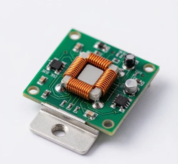
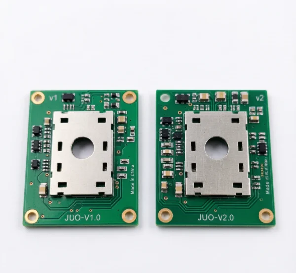
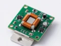
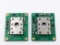
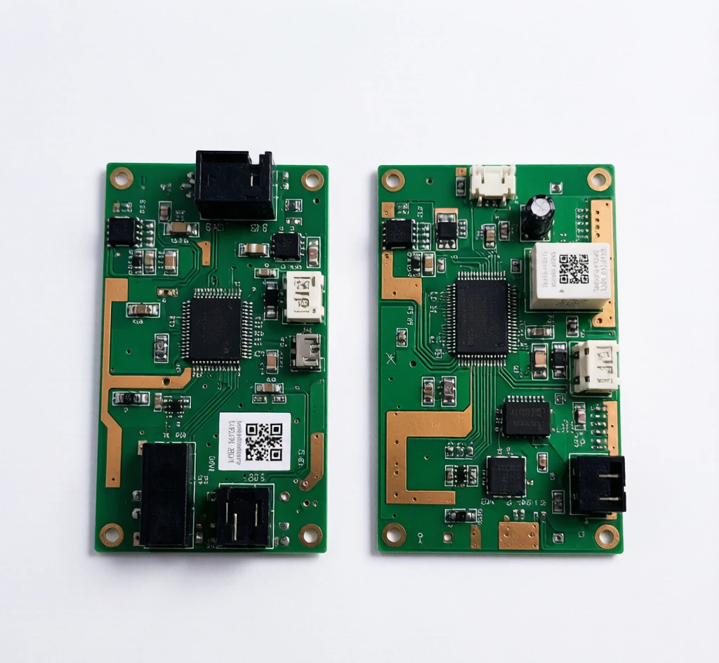
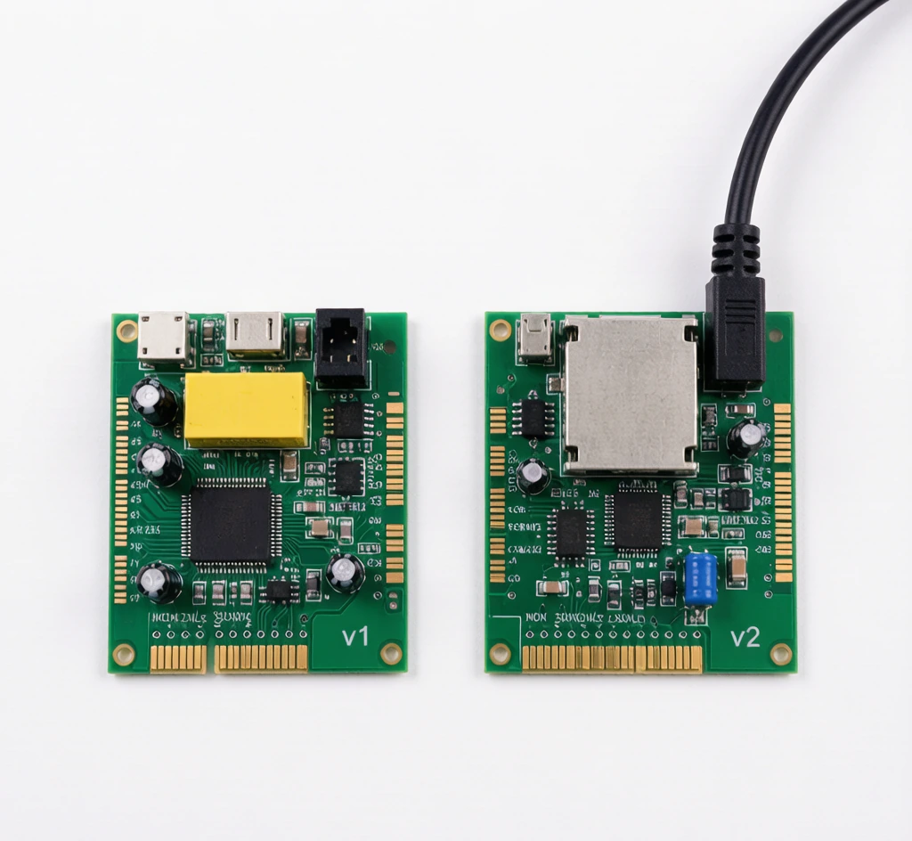
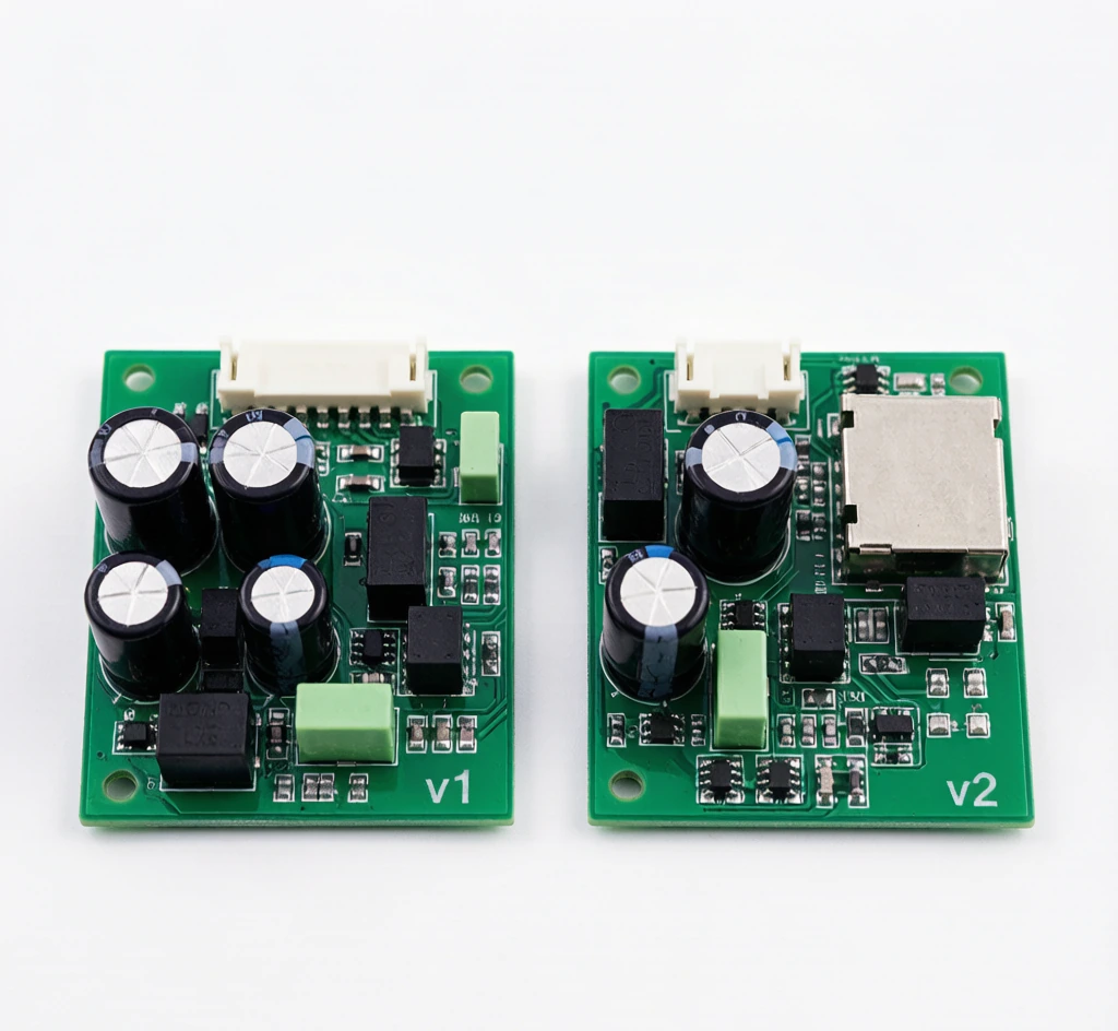
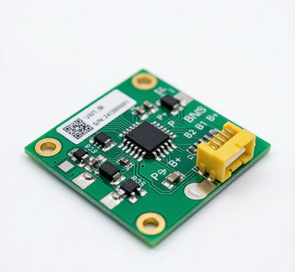
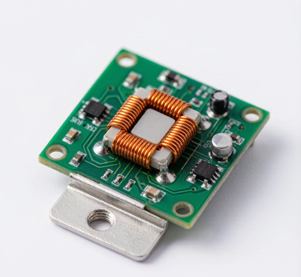
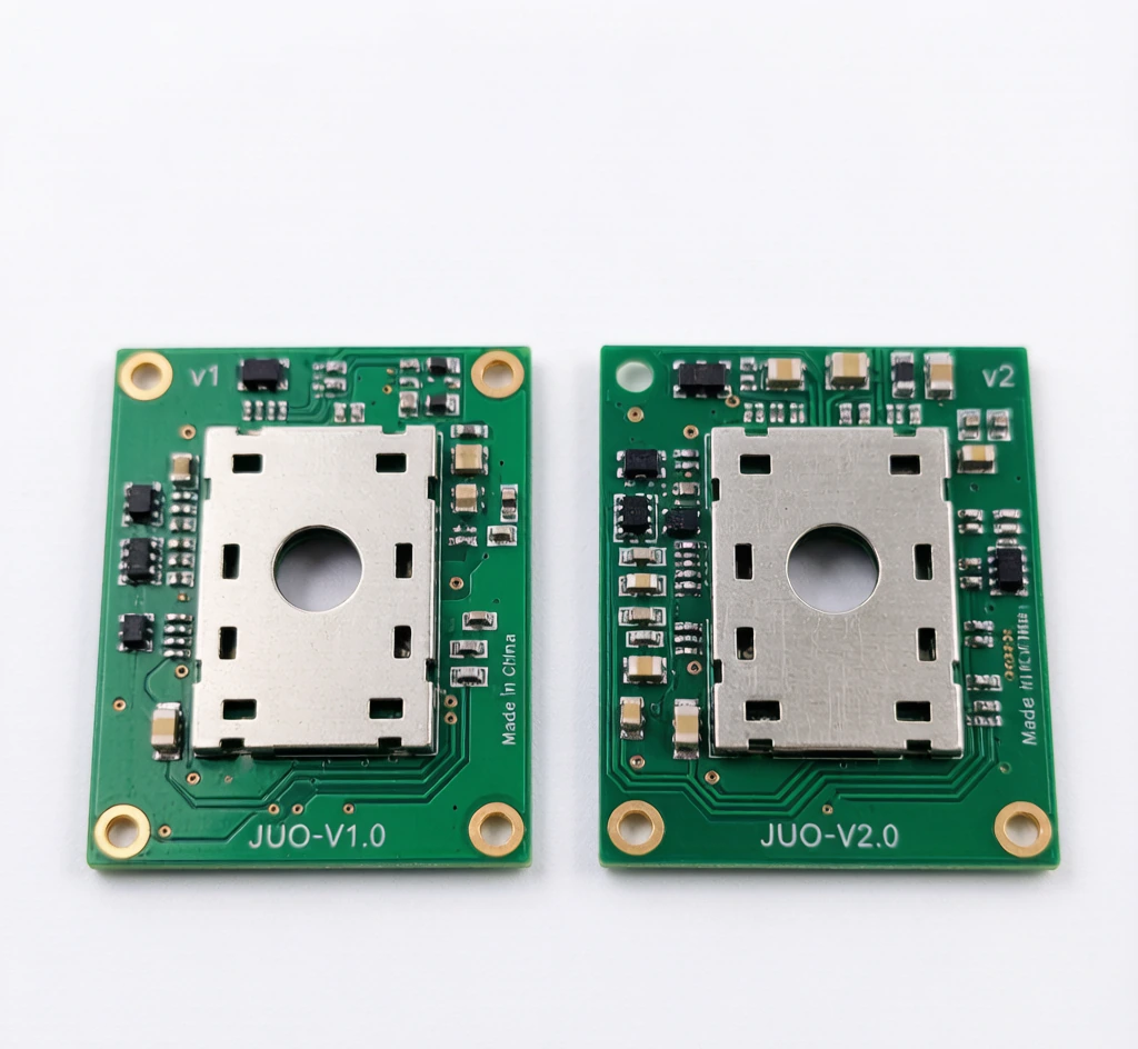
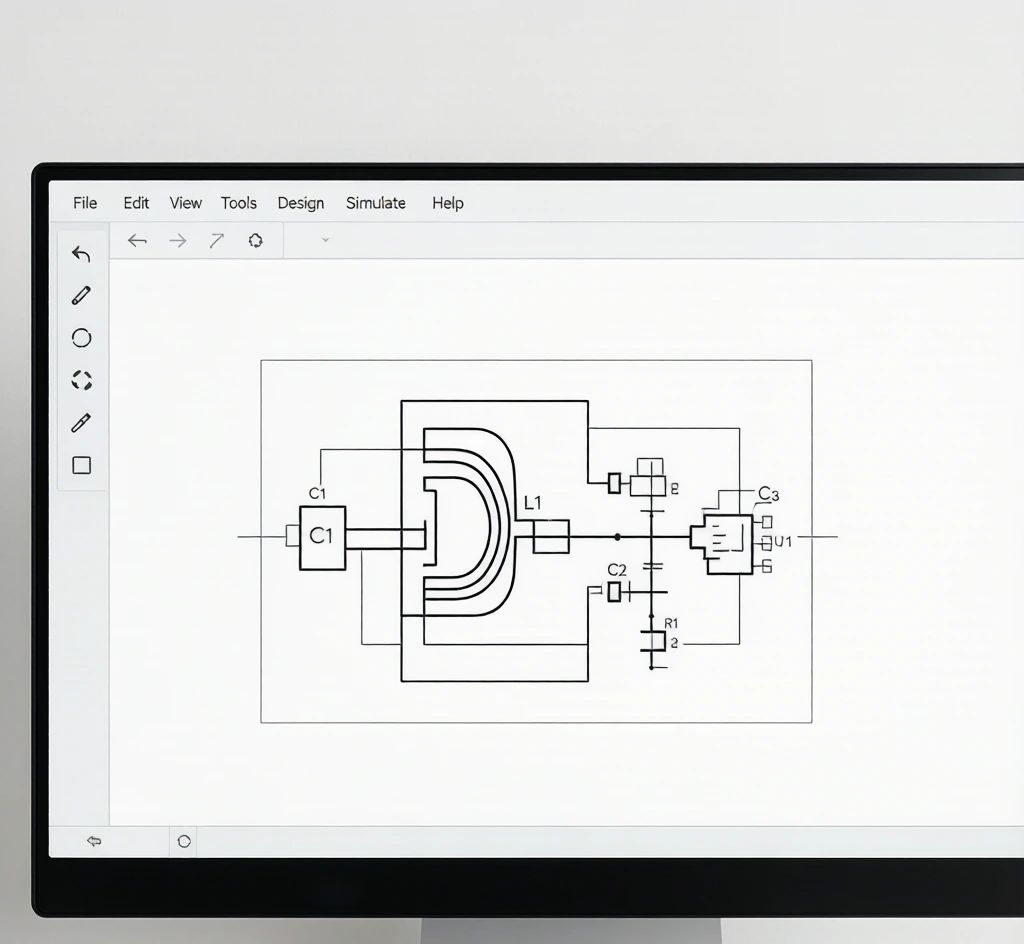
This OEM/ODM project demonstrates the hardware development of a Qi wireless charging module PCBA for integration into consumer electronics and automotive accessories. The reference design provides 15 W wireless charging with a single-coil architecture on a compact 50 × 40 mm board. Development focuses on coil matching, power-conversion efficiency, foreign-object detection (FOD) and over-temperature protection (OTP) for customized wireless charging applications.
2. Qi Wireless Charging Hardware Development
• Qi Wireless Charging: The reference module is developed around the Qi wireless charging standard for compatible receiving devices.
• 15 W Power Output: The demonstrated hardware provides up to 15 W wireless charging power according to the reference project configuration.
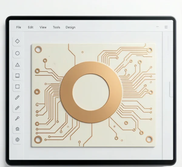
• Single-Coil Architecture: Uses a single transmitting coil within the specified wireless charging hardware design.
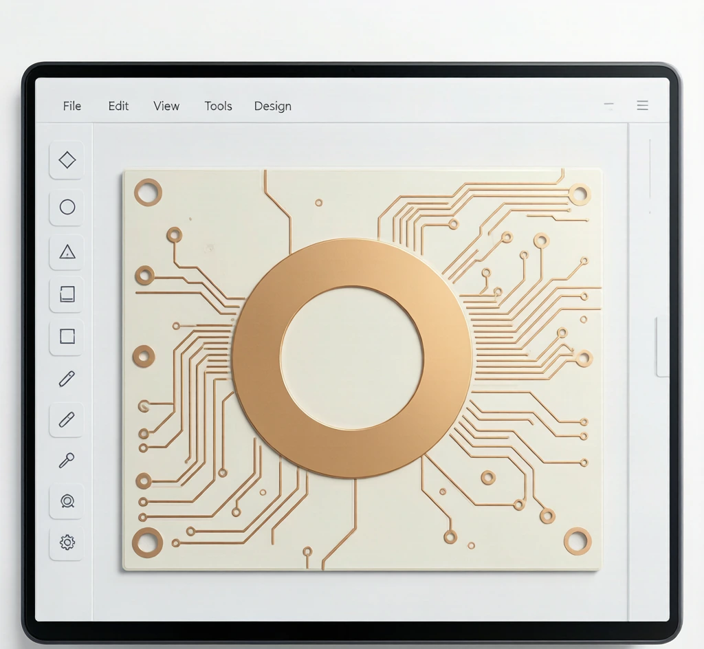
• Coil Matching Optimization: Coil and circuit parameters are matched during development to support stable power transfer and charging performance.
• Compact PCB Design: The 50 × 40 mm reference board demonstrates integration of wireless charging circuitry within space-constrained products.
3. Power Efficiency & Circuit Optimization
• ≥75% Reference Efficiency: The demonstrated project specifies power-conversion efficiency of at least 75% under its defined operating conditions.
• Power Circuit Development: Charging and power-control circuitry is developed around the required wireless charging architecture.
• Hardware Parameter Optimization: Circuit parameters can be adjusted during prototype development according to coil characteristics and charging requirements.
• System Integration: The PCBA can be developed around the customer’s enclosure, coil arrangement and complete charging-product architecture.
4. FOD & Thermal Protection
• Foreign-Object Detection: FOD circuitry is incorporated to detect applicable foreign objects within the wireless charging area.
• Over-Temperature Protection: OTP circuitry provides thermal protection according to the defined hardware design and operating thresholds.
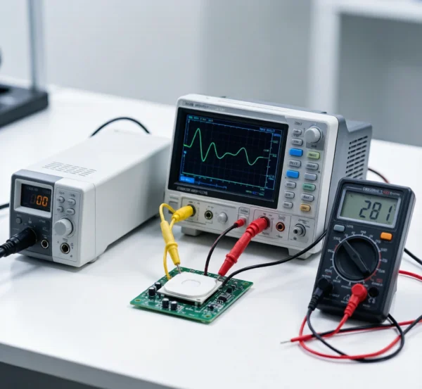
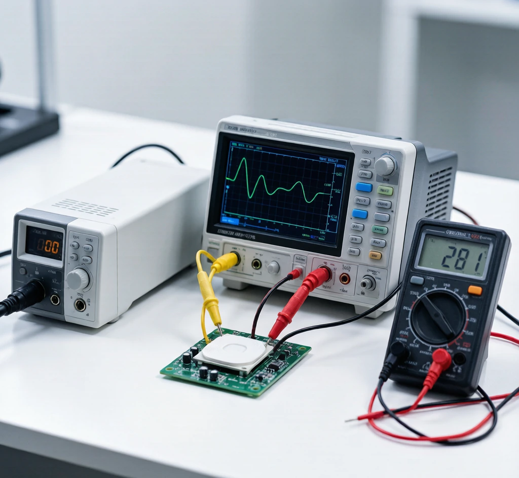
• Protection Circuit Verification: FOD and OTP functions can be evaluated during hardware debugging and prototype validation.
• Thermal Performance Evaluation: Charging behavior and temperature conditions can be reviewed during development to support reliable system integration.
5. OEM/ODM Development Capability
• Project-Based Wireless Charging Development: Board dimensions, charging power, coil configuration and protection functions can be developed according to customer requirements.
• Coil & PCBA Integration: Supports coordinated development of the charging coil, matching circuitry and control hardware.
• Multiple Product Applications: Development capability can support desktop, consumer-electronics and in-vehicle wireless charging projects.
• Hardware-to-Production Support: Covers PCB hardware development, circuit optimization, debugging and production introduction according to project scope.
Applications
• Smartphone wireless charging pads
• Desktop wireless charging modules
• In-vehicle wireless charging mounts
• Embedded wireless charging devices
• Consumer electronics charging products
• Custom Qi wireless charging projects
Package
• Reference PCBA Size: 50 × 40 mm
• Reference Net Weight: Approx. 15 g/board
• Individual Packaging: ESD vacuum-sealed moisture-barrier bag with desiccant
• Quantity per Bag: 5 pcs
• Master Carton Dimensions: 320 × 260 × 200 mm
• Quantity per Master Carton: 500 pcs
• Gross Weight per Master Carton: Approx. 8.5 kg
• Packaging is designed for ESD-sensitive PCBA transportation.