1. Project Overview
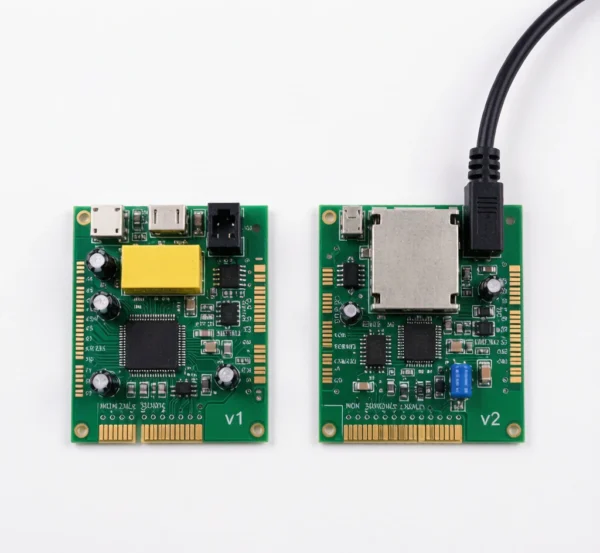
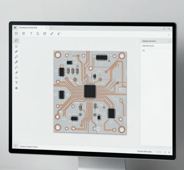
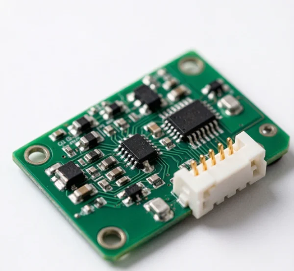
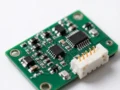
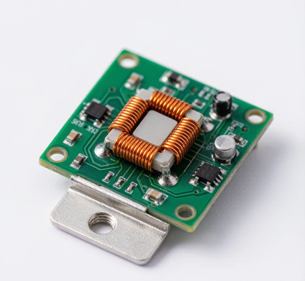
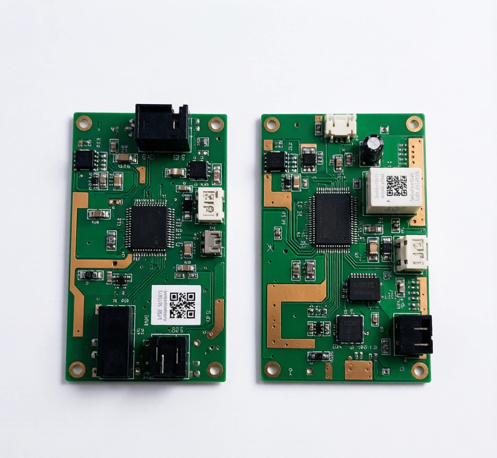
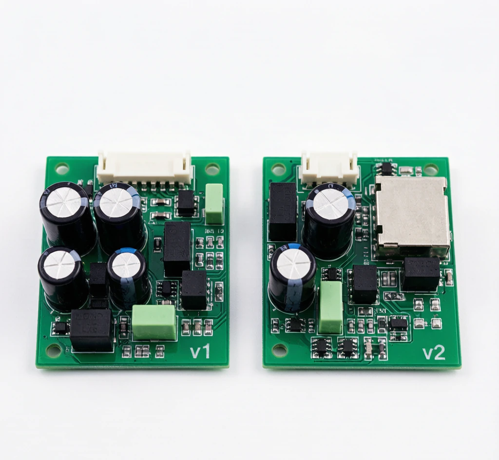
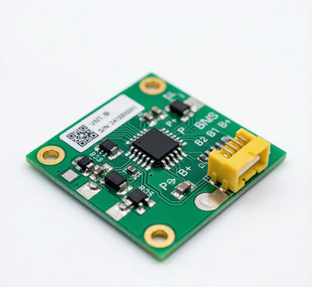
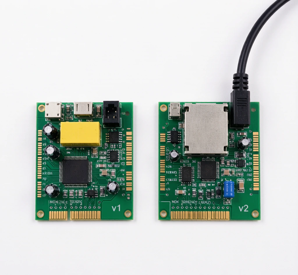
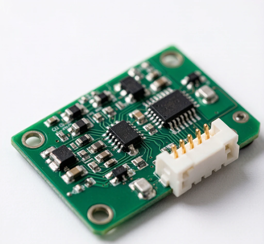
This OEM/ODM project demonstrates the hardware development of a main control PCBA for smart home and IoT devices. The reference design uses a compact 4-layer, 70 × 50 mm PCB integrating WiFi + Bluetooth wireless connectivity, I2C/SPI peripheral interfaces and low-power design. The development process covers wireless and peripheral circuit integration, hardware debugging and production ramp-up for customized smart-home electronics.
2. Wireless & Control Hardware Development
• WiFi + Bluetooth Connectivity: The reference board integrates WiFi and Bluetooth communication for connection with compatible smart-home devices, gateways and user terminals.
• 4-Layer PCB Design: Uses a four-layer PCB architecture to accommodate control, wireless and peripheral circuitry within the compact board dimensions.
• Peripheral Circuit Integration: Supporting circuits can be matched and developed around the main control architecture and connected device requirements.
• I2C / SPI Interfaces: Provides standard peripheral interfaces for compatible sensors, controllers and other electronic components.
• Compact Board Layout: The 70 × 50 mm reference design demonstrates hardware integration for space-constrained smart-home products.
3. Low-Power & IoT Integration
• Low-Power Design: Hardware architecture is developed with power consumption requirements in mind for compatible smart-home and IoT applications.
• Sensor Integration: Peripheral interfaces can support integration with compatible sensing components according to the customer’s product architecture.
• Smart Device Control: The PCBA can serve as the main hardware control platform for connected switches, plugs, gateways and other IoT devices.
• Wireless System Integration: Wireless communication circuitry is coordinated with the main controller and peripheral hardware during board development.
4. Hardware Debugging & Production Ramp-Up
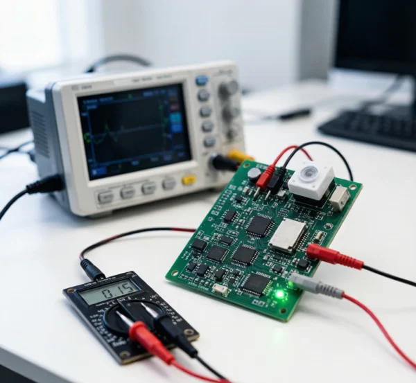
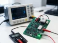
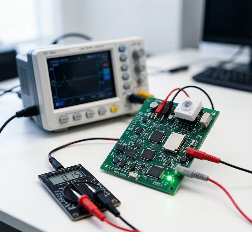
• Hardware Debugging: Prototype boards are tested and adjusted to verify core circuits, interfaces and wireless hardware operation.
• Functional Verification: Key board functions can be evaluated against the electrical and system requirements defined for the project.
• Design Optimization: Findings from prototype debugging can be incorporated into subsequent PCB and circuit revisions.
• Production Ramp-Up: Hardware development supports the transition from validated board design to repeatable PCBA manufacturing.
• FCC / CE Support: The reference project was developed with FCC/CE certification requirements in mind; final certification depends on the completed product and applicable testing.
5. OEM/ODM Development Capability
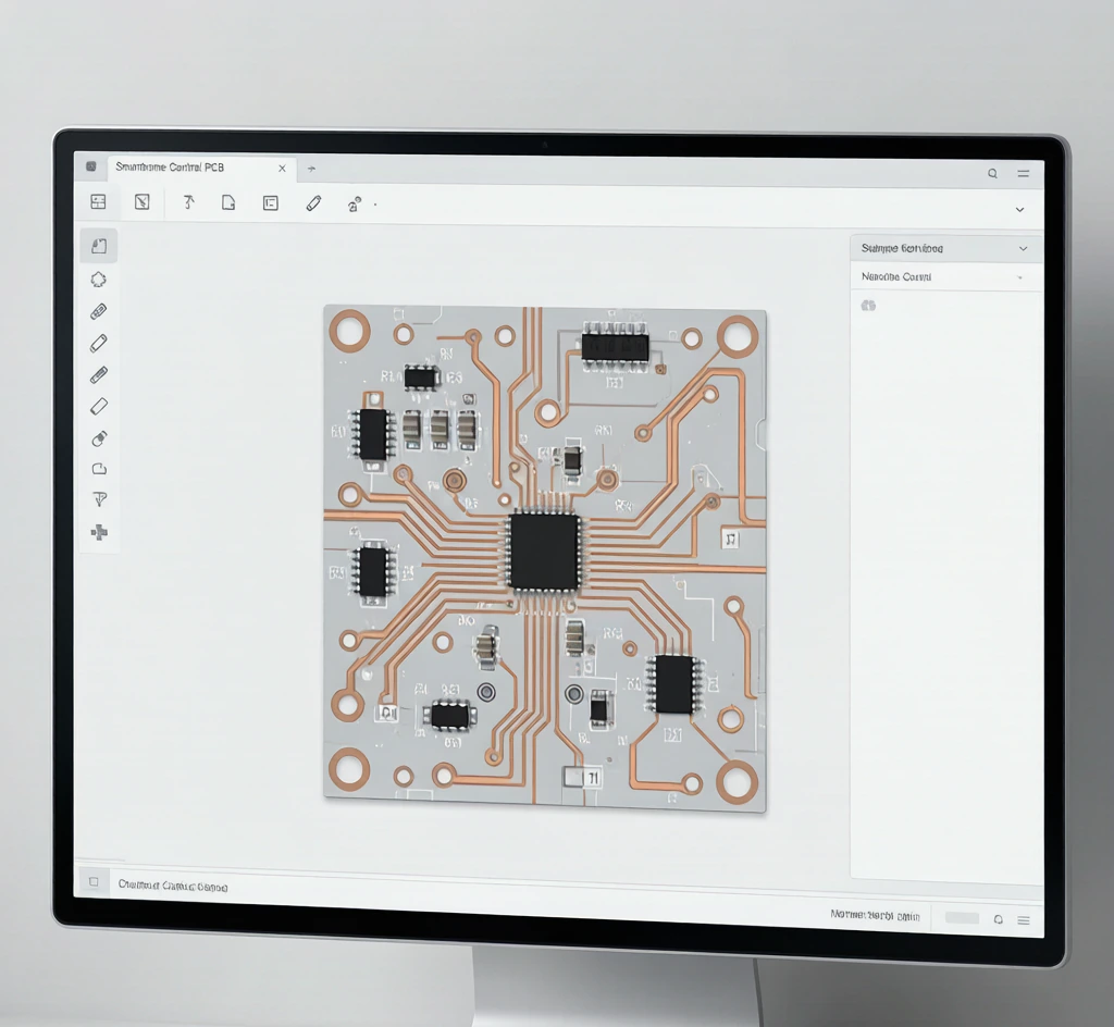
• Project-Based PCBA Development: Board dimensions, wireless configuration, interfaces and peripheral circuits can be developed according to individual customer requirements.
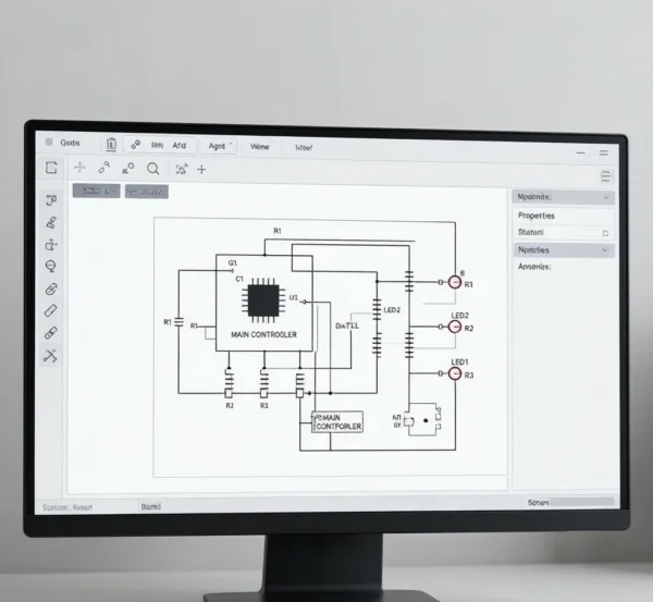
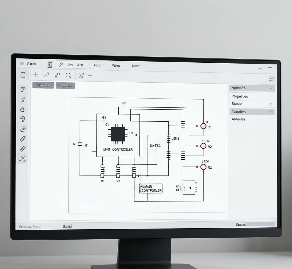
• Hardware-to-Production Support: Supports schematic and PCB development, hardware debugging and production introduction according to project scope.
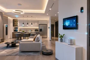
• Smart Home Product Applications: Development capability can be applied across multiple connected-home and IoT device categories.
• Custom Hardware Integration: PCBA architecture can be developed around the customer’s enclosure, sensors, communication requirements and overall product system.
Applications
• Smart switches
• Smart plugs
• Smart home gateways
• IoT sensor nodes
• Connected home controllers
• Wireless smart-home devices
• Custom IoT hardware projects
Package
• Reference PCBA Size: 70 × 50 mm
• Reference Net Weight: Approx. 25 g/board
• Individual Packaging: ESD vacuum-sealed moisture-barrier bag with desiccant
• Quantity per Bag: 1 pc
• Master Carton Dimensions: 360 × 280 × 220 mm
• Quantity per Master Carton: 200 pcs
• Gross Weight per Master Carton: Approx. 6.2 kg
• Packaging is designed for ESD-sensitive PCBA transportation.