1. Project Overview
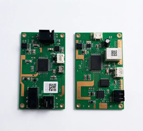
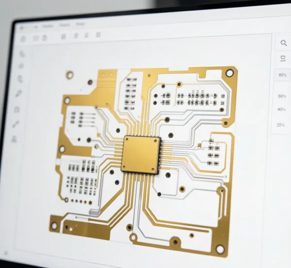
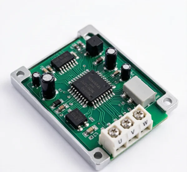
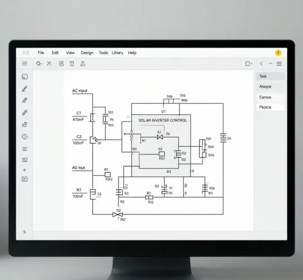
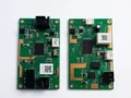
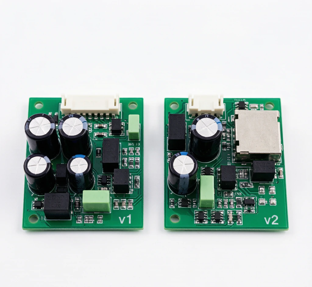
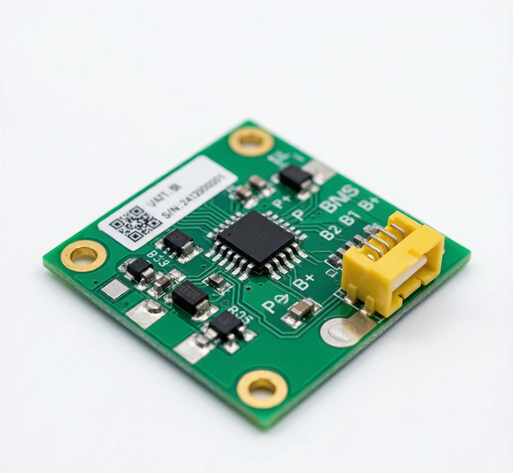
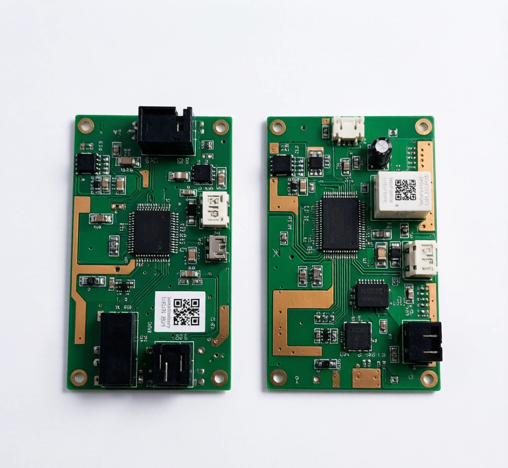
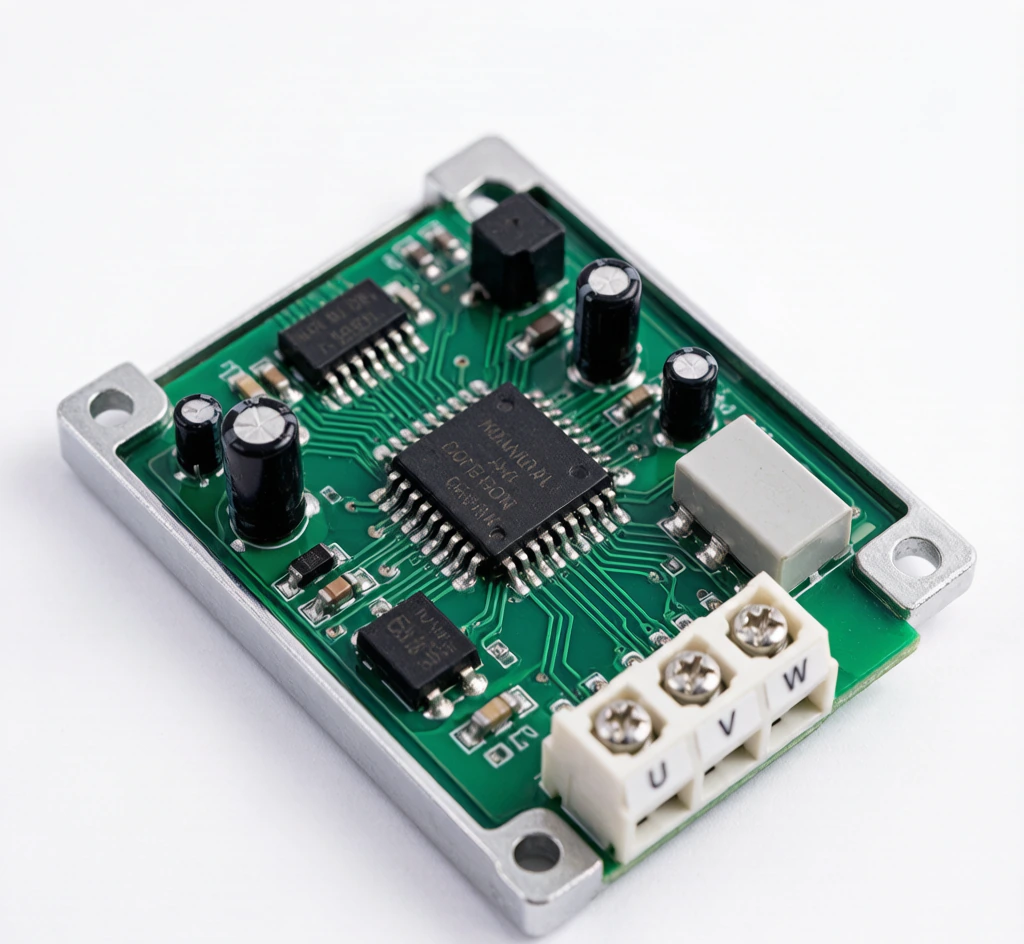
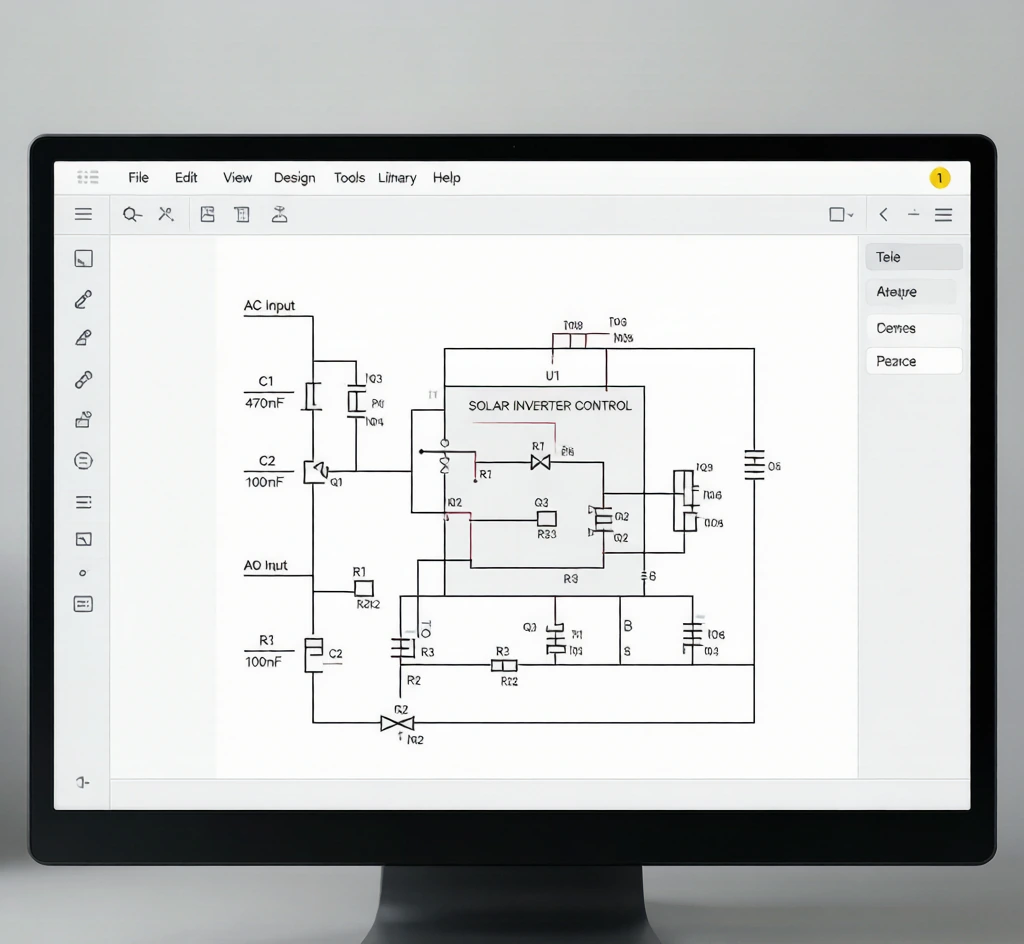
This OEM/ODM project demonstrates the hardware development of an inverter control PCBA for power conversion systems. The reference design uses a 6-layer, 150 × 100 mm PCB with full-bridge topology, isolated gate drive, current and voltage sensing, and multi-level protection. Development covers power-drive and sensing circuit design, hardware parameter calibration and system-level commissioning for customized inverter applications.
2. Power Drive & Control Design
• Full-Bridge Topology: The reference design uses a full-bridge architecture for power conversion and inverter control.
• Isolated Gate Drive: Provides electrical isolation between the control and power switching sections according to the reference inverter architecture.
• Power-Drive Circuit Design: Gate-drive and related control circuits are developed around the selected switching devices and system requirements.
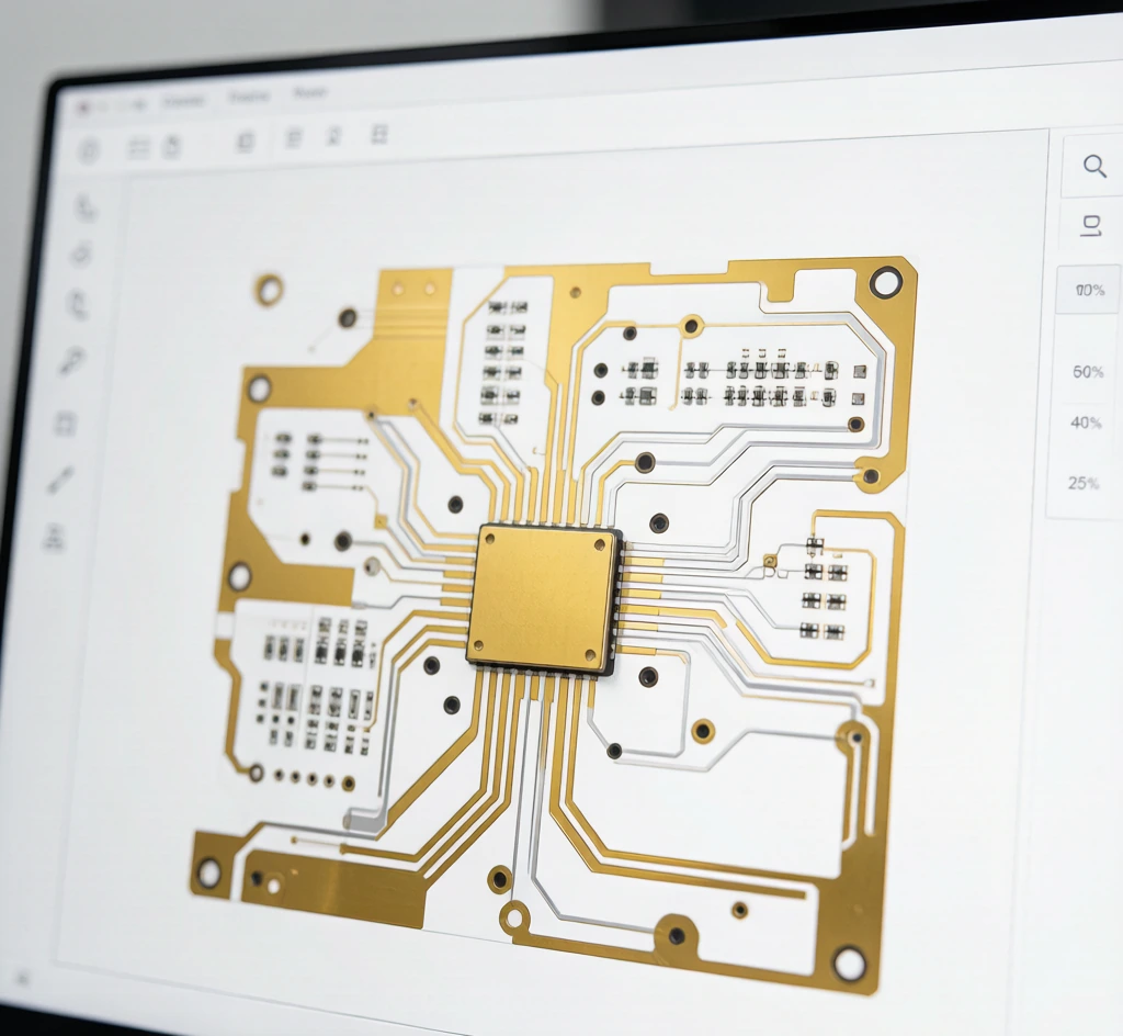
• 6-Layer PCB Architecture: The reference board uses a six-layer PCB structure to integrate control, sensing and drive circuitry within the specified board dimensions.
• Hardware Parameter Calibration: Key circuit parameters are calibrated during development according to the electrical requirements of the inverter system.
3. Current & Voltage Sensing
• Current Sensing: Monitors relevant current signals required for inverter control, feedback and protection functions.
• Voltage Sensing: Provides voltage feedback for compatible control and system-monitoring functions.
• Signal Conditioning: Sensing signals can be conditioned according to the requirements of the control circuitry and measurement range.
• Feedback Integration: Current and voltage feedback circuits are integrated with the control architecture for system-level operation.
4. Protection & System Commissioning
• Multi-Level Protection: The reference hardware incorporates multiple protection functions according to the defined inverter system requirements.
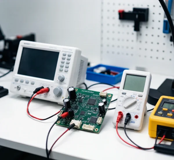
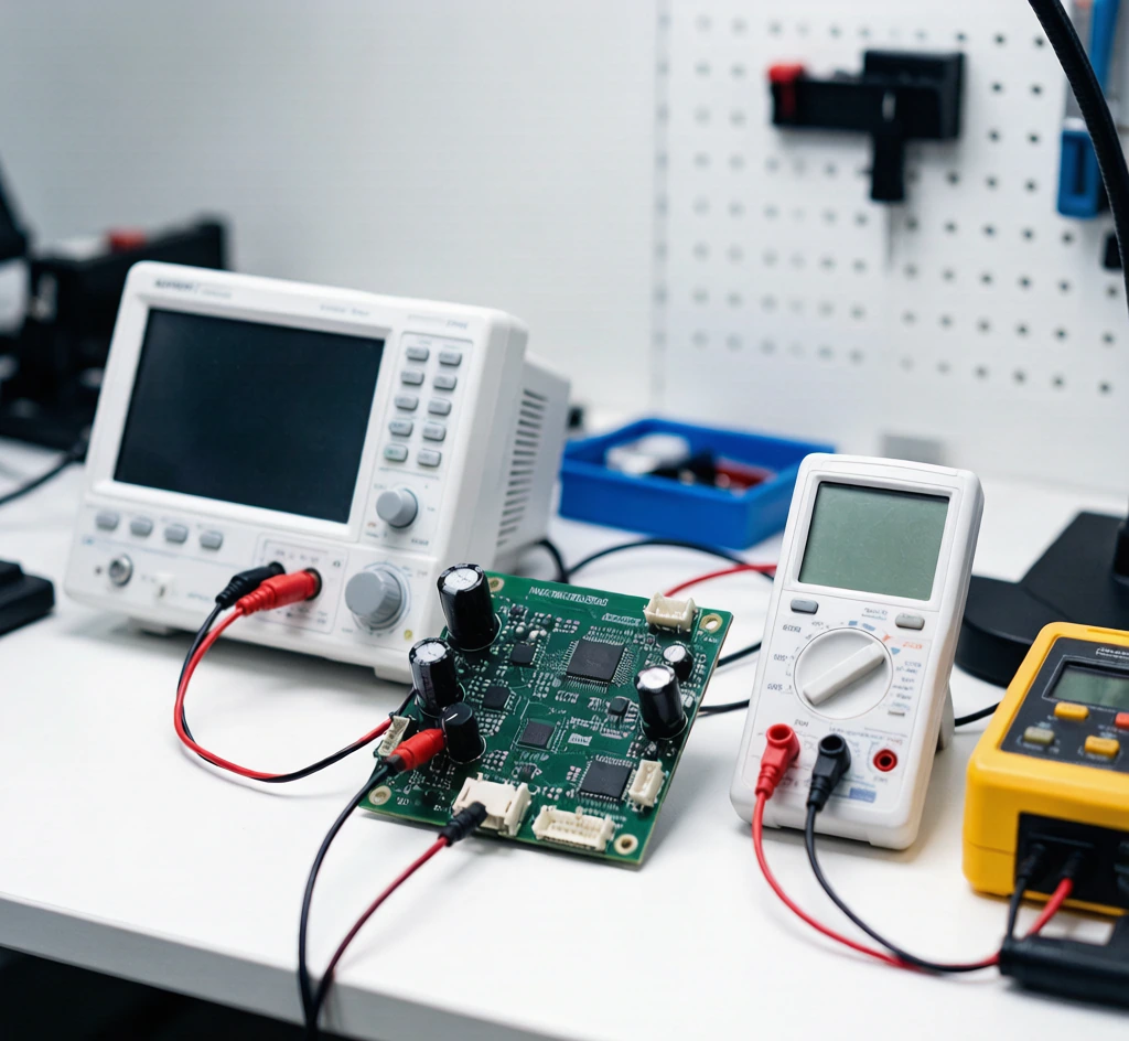
• Hardware Verification: Prototype boards are evaluated to verify drive, sensing and protection circuitry before production introduction.
• System-Level Commissioning: The control board is tested together with the corresponding inverter hardware to evaluate integrated system operation.
• Design Optimization: Findings from hardware testing and system commissioning can be incorporated into subsequent circuit and PCB revisions.
• Production Validation: The finalized hardware can proceed through verification before transition to repeatable PCBA manufacturing.
5. OEM/ODM Development Capability
• Project-Based Inverter Development: Board architecture, topology, gate-drive circuits, sensing and protection functions can be developed according to customer requirements.
• Power Electronics Integration: Supports coordination of control, drive, sensing and protection circuitry within customized inverter projects.
• Multiple Inverter Applications: Development capability can support portable energy storage, residential solar and vehicle inverter projects.
• Hardware-to-System Support: Covers circuit development, PCB implementation, hardware calibration and system-level commissioning according to project scope.
Applications
• Portable energy storage inverters
• Residential solar inverter systems
• Vehicle power inverters
• DC-to-AC power conversion systems
• Energy storage power electronics
• Custom inverter hardware projects
Package
• Reference PCBA Size: 150 × 100 mm
• Reference Net Weight: Approx. 120 g/board
• Individual Packaging: ESD vacuum-sealed moisture-barrier bag with desiccant
• Quantity per Bag: 1 pc
• Master Carton Dimensions: 500 × 350 × 300 mm
• Quantity per Master Carton: 30 pcs
• Gross Weight per Master Carton: Approx. 4.8 kg
• Packaging is designed for ESD-sensitive PCBA transportation.